The electric connection on a PCB depends on the conductivity of
copper. As an active chemical substance, however, copper tends to
be oxidized when being exposed to atmospheric humidity, thereafter
leading to issues that will possibly take place in high-temperature
soldering, which badly threatens components' solid fixation on PCBs
and reduces reliability of end products. Therefore,
Surface finish carries two key responsibilities when it comes to the performance
of PCBs: to protect copper from being oxidized and to provide a
surface for high solderability when components are ready to be
assembled on PCBs.
Board finishes can be classified into different classifications
based on different technologies and involved chemical substances:
HASL (hot air soldering leveling), Immersion Tin/Silver, OSP,
ENIG and ENEPIG, etc. Among all the finishes, OSP is becoming increasingly
prevalent owing to its low cost and environment-friendly
attributes, which adds more necessity for us to better understand
it. That's what this article aims to tell you.
Brief Introduction of OSP
OSP is short for "organic solderability preservatives", and it's
also called anti-tarnish. It refers to a layer of organic finish
generated on clean and bare copper by adsorption. On the one hand,
this organic finish is capable of stopping copper from being oxide,
thermal shock or moisture. On the other hand, it has to be easily
eliminated by flux in the later process of soldering so that the
exposed clean copper can be jointed with melting solder so that
solder joints can be generated in extremely short time.
The applied water-based chemical compound belongs to azole family
such as benzotriazoles, imidazoles, and benzimidazoles, all of
which get adsorbed on the copper surface with coordination formed
between them and copper atoms, leading to the production of film.
In terms of film thickness, film made through benzotriazoles is
thin while that through imidazoles is relatively thick. The
differentiation on thickness will bring distinct impact to effect
of board finish which will be discussed in the later part of this
article.
Manufacturing Process of OSP
Actually, OSP has a decade's history which is longer than that of
SMT (Surface Mount Technology). Here's OSP's manufacturing process.
 | PCBCart")
Note: DI refers to deionization.
The function of "Clean" is to clean off the organic contaminants
such as oil, finger prints, oxidation film etc. so as to get copper
foil surface stay clean and bright, which is the fundamental
demand. This step plays quite a crucial role in preservatives build
quality. Bad cleaning will tend to cause uneven thickness of
preservatives build. In order to ensure the high quality of
finished OSP film, on the one hand, concentration of cleaning
solution should be controlled within a standard range through
chemical laboratory analysis. On the other hand, cleaning effect is
advised to be checked as often as possible and once the effect
doesn't reach the standard, cleaning solution should be instantly
replaced.
In the process of Topography enhancement, micro etching is usually
applied to substantially eliminate the oxidation generated on
copper foil so that the bonding forces can be improved between
copper foil and OSP solution. The speed of micro etching directly
influences the film build rate. Thus, in order to obtain smooth and
even film thickness, it's critical to keep the stability of micro
etching speed. Generally speaking, it's suitable to control the
micro etching speed in the range from 1.0 to 1.5μm per minute.
It's best that DI rinse is utilized before preservatives build in
case OSP solution will be polluted by other ions, which leads to
tarnish after reflow solder. Similarly, it's best that DI rinse
should be utilized after preservatives build with the PH value
between 4.0 and 7.0 in case preservatives would be destroyed as a
result of pollution.
Advantages of OSP
Nowadays, OSP has been usually applied due to its advantages that
are discussed below:
• Simple manufacturing process and Reworkable: Circuit boards coated with OSP can be easily reworked by PCB
fabricators so that PCB assemblers are allowed to have fresh
coatings once its coating is found damaged.
• Good wettability: OSP-coated boards perform better in terms of solder wetting when
flux meets vias and pads.
• Environment friendly: Since water-based compound is applied in the process of OSP
generation, it does no harm to our environment, just falling into
people's expectations for green world. As a result, OSP is an
optimal selection for electronic products catering to green
regulations such as
RoHS.
• Low cost: Due to the simple chemical compounds applied in OSP creation and
its easy manufacturing process, OSP stands out in terms of cost
among all types of surface finishes. It costs less, leading to a
lower cost of circuit boards in the end.
• Fit for reflow soldering in double-side SMT assembly: Along with the constant development and progress of OSP, it has
been accepted from single-sided SMT assembly to double-sided SMT
assembly, dramatically widening its application fields.
• Low requirement for solder mask ink
• Long storage time

Get an Instant Quote on OSP PCBs
Storage Requirement of PCBs Coated with OSP
Since the preservative generated by OSP technology is so thin and
easy to be cut, much care must be taken in the process of operation
and transportation. PCBs with OSP as surface finish are exposed to
high temperature and humidity for such a long time that oxidation
will be possibly generated on the surface of PCBs, thereafter
leading to low solderability. Therefore, storing methods must stick
to these principles:
a. Vacuum package should be utilized with desiccant and humidity
display card. Put release paper between PCBs to stop friction
destroying PCB surface.
b. These PCBs can't be directly exposed to the sunlight. The
requirements of optimal storage environment include: relative
humidity (30-70%RH), temperature (15-30°C) and storage time (fewer
than 12 months).

Possible Problem of OSP after Soldering
Sometimes, the color of OSP boards changes after soldering, which
mainly has something to do with preservatives thickness, micro
etching quantity, soldering times and even abnormal contaminants.
Luckily, this probelem can be observed just from the appearance.
Usually, there are two circumstances:

For Circumstance#1, in the process of soldering, flux is capable of
helping eliminating oxidations so that soldering performance won't
be influenced. Accordingly, no more measurements have to be taken.
On the contrary, Circumstance#2 occurs because OSP integrity has
been destroyed so that flux isn’t capable of eliminating
oxidations, which will greatly decrease the soldering performance.
Therefore, following improvements and measurements must be taken to
ensure the appearance and performance of organic solderability
preservatives surface finish:
a. The thickness of OSP must be controlled within a certain range;
b. The amount of micro-etching must be controlled within a certain
range;
c. During PCB fabrication, contaminants (gel residue, ink etc.) must
be 100% eliminated in case partial abnormity or badly-performed
solderability occurs.
PCBCart Provides You the Best
PCBCart provides quick-turn prototype PCBs compatible with IPC1 and
standard PCBs with standard IPC2 with short turn time. High quality
and low cost have been our business core since our establishment 14
years ago. Up to now, we've won a customer satisfaction rate as
high as 99% from more than 10,000 customers around the globe.
AND, you will be one of them.
Try PCB Prototype Quote
PCB Fab Quote Online
Helpful Resources
•
Detailed Introduction on PCB Surface Finishes and Their
Applications
•
The Most Comprehensive Guidelines for Surface Finish Selection
•
Full Feature Custom PCB Manufacturing Service from China's Most
Experienced Fab House
•
Guide on Getting PCB Fabrication Price within Seconds
•
File Requirements for a Quick And Efficient PCB Fabrication
Description


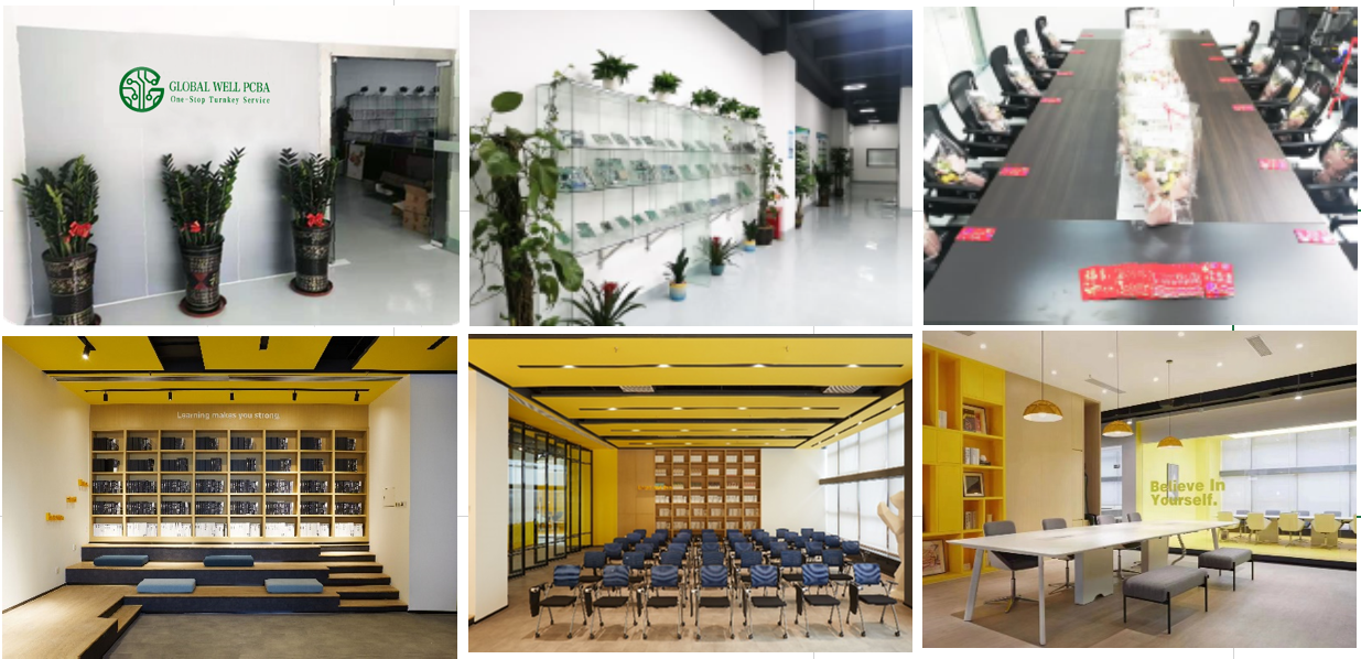
Company Information
Global Well Electronic Inc. is a professional PCB solution supplier
from Shenzhen, China, integrating PCB circuit board production and
processing, STM processing and mounting, PCBA OEM, component
purchasing, PCB/PCBA custom design-production- A comprehensive PCB
circuit board company with one-stop turnkey service of
processing-assembly-finished products. The company has a strong
supply chain system, a professional and efficient collaborative
team, a sound and complete quality control system, and the business
philosophy of honesty and trustworthiness, customer first, and
presents the products to everyone with low prices, reliable
quality, high-quality service and after-sales service. client.
We provide total PCB solutions from PCB design to final mass
production, including PCB fabrication and assembly, component
sourcing, solder paste stencils, conformal coatings, and more.
Serving the global electronics field, including industrial control,
medical electronics, military equipment, power communication,
automotive electronics, AI artificial intelligence, smart home and
other industries.

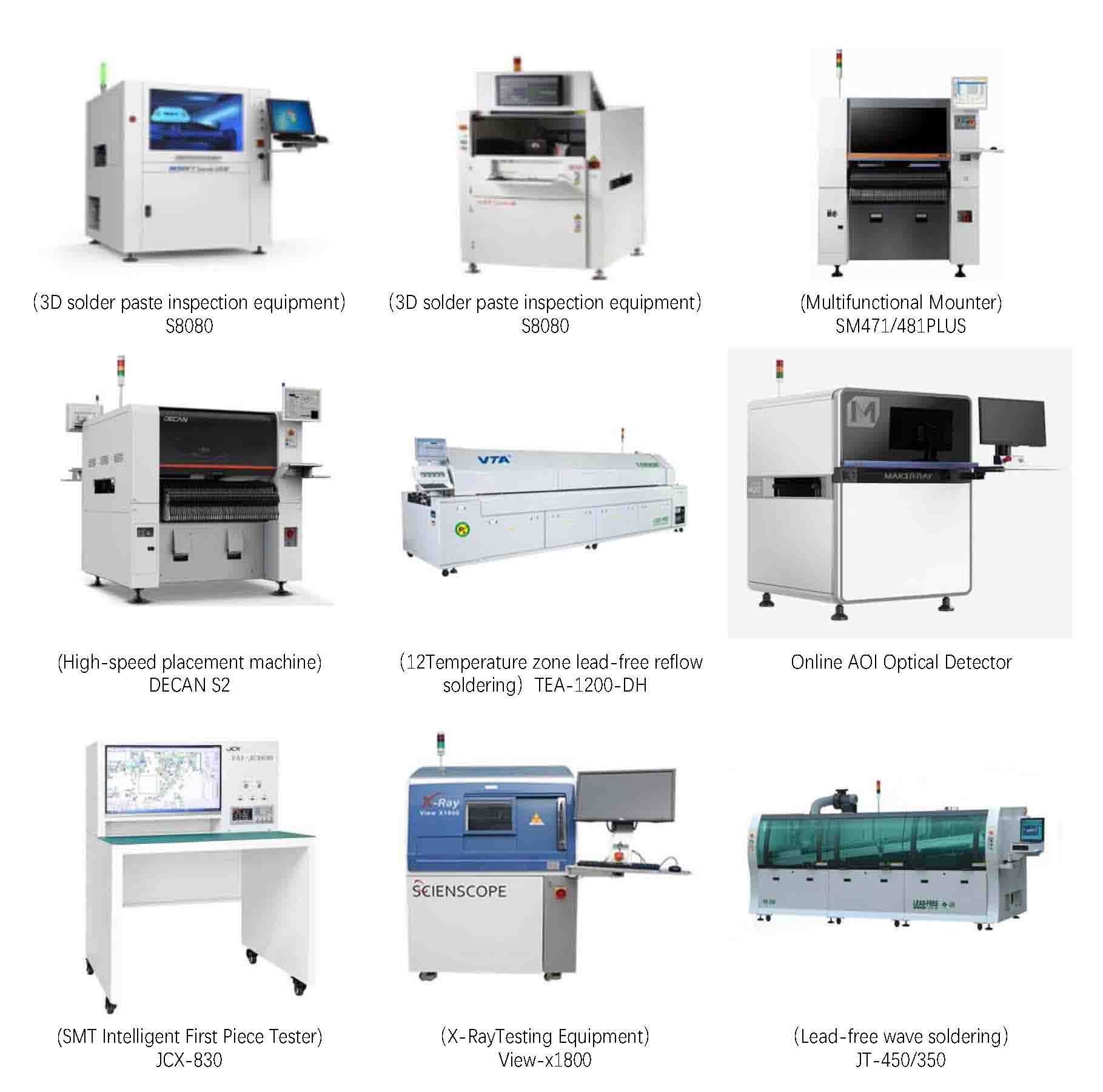
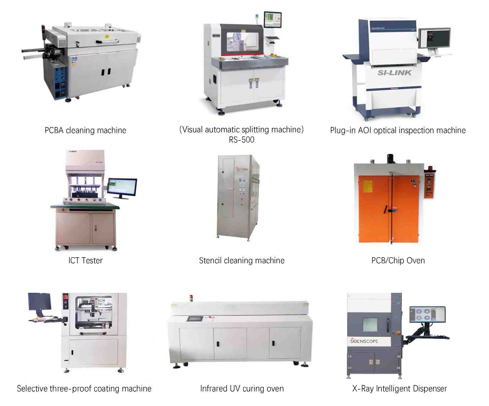
Our factory located in Shenzhen, and have almost 300 employees,
more than 30 production lines include SMT, DIP, automatic welding,
aging test and assembly. We have SMT machines from Japan and Korea,
automatic solder paste printing machines, solder paste inspection
machine(SPI)12 temperature zone reflow soldering machine, AOI
detector, X-RAY detector, wave soldering machine, EM PCB
,dispenser,laser print machine etc., Different line configurations
can meet requirements from small sample order to bulk shipment.
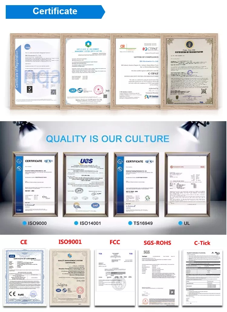
Our company has obtained ISO 9001 quality system certification and
ISO 14001 system certification. With multi-testingprocedures, our
products carry out the quality system standard strictly.
1. PCB fabrication.
2. Turnkey PCBA: PCB+components sourcing+SMD and through-hole
assembly
3. PCB clone, PCB reverse engineering.

PCB or PCBA Files Requests:
1. Gerber files of the bare PCB board
2. BOM (Bill of material) for assembly (please kindly advise us if
there is any acceptablecomponents substitution.)
3. Testing Guide & Test Fixtures if necessary
4. Programming files & Programming tool if necessary
5. Schematic if necessary

PCB Technical Specification
(1) PCB Technical Specification
| Order Quantity | 1-300,000,30000 Square Meter/Square Meters per Month module
electronic board |
| Layer | 1,2,4,6,upto 40 layer |
| Material | FR-4,glass epoxy,FR4 High Tg,Rohs compliant,Aluminum,Rogers,etc |
| PCB type | Rigid,flexible,rigid-flexible |
| Shape | Any shape: Rectangular,round,slots,cutouts,complex,irregular |
| Max PCB dimensions | 20inch*20inch or 500mm*500mm |
| Thickness | 0.2~4.0mm, Flex 0.01~0.25'' |
| Thickness tolerance | ± 10% |
| Copper thickness | 0.5-4 oz |
| Copper thickness tolerance | ± 0.25oz |
| Surface finish | HASL,Nickle,Imm Gold,Imm Tin,Imm Silver,OSP etc |
| Solder mask | Green, red,white,yellow,blue,black, Double-sided |
| Silk screen | White,yellow,black,or negative, Double-sided or single-sided |
| Silk screen min line width | 0.006'' or 0.15mm |
| Min drill hole diameter | 0.01'',0.25mm.or 10 mil |
| Min trace/gap | 0.075mm or 3mil |
| PCB cutting | Shear,V-score,tab-routed |
(2) Turnkey PCBA Capabilities
| Turnkey PCBA | PCB+components sourcing+assembly+package |
| Assembly details | SMT and Thru-hole, ISO lines |
| Lead Time | Prototype: 15 work days. Mass order: 20~25 work days |
| Testing on products | Flying Probe Test, X-ray Inspection, AOI Test, functional test |
| Quantity | Min quantity: 1pcs. Prototype, small order, mass order, all OK |
| Files we need | PCB: Gerber files(CAM, PCB, PCBDOC) |
| Components: Bill of Materials(BOM list) |
| Assembly: Pick-N-Place file |
| PCB panel Size | Min size: 0.25*0.25 inches(6*6mm) |
| Max size: 20*20 inches(500*500mm) |
| PCB Solder Type | Water Soluble Solder Paste, RoHS lead free |
| Components details | Passive Down to 0201 size |
| BGA and VFBGA |
| Leadless Chip Carriers/CSP |
| Double-sided SMT Assembly |
| Fine Pitch to 0.8mils |
| BGA Repair and Reball |
| Part Removal and Replacement |
| Component package | Cut Tape,Tube,Reels,Loose Parts |
| PCBA process | Drilling-----Exposure-----Plating-----Etaching Stripping-----Punching-----Electrical Testing-----SMT-----Wave Soldering-----Assembling-----ICT-----Function
Testing-----Temperature - Humidity Testing |
Main Equipment:

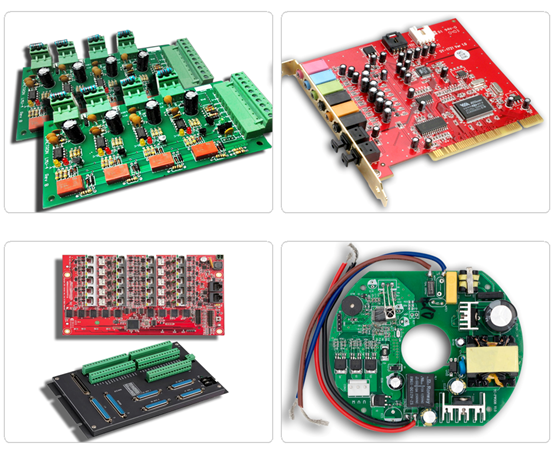
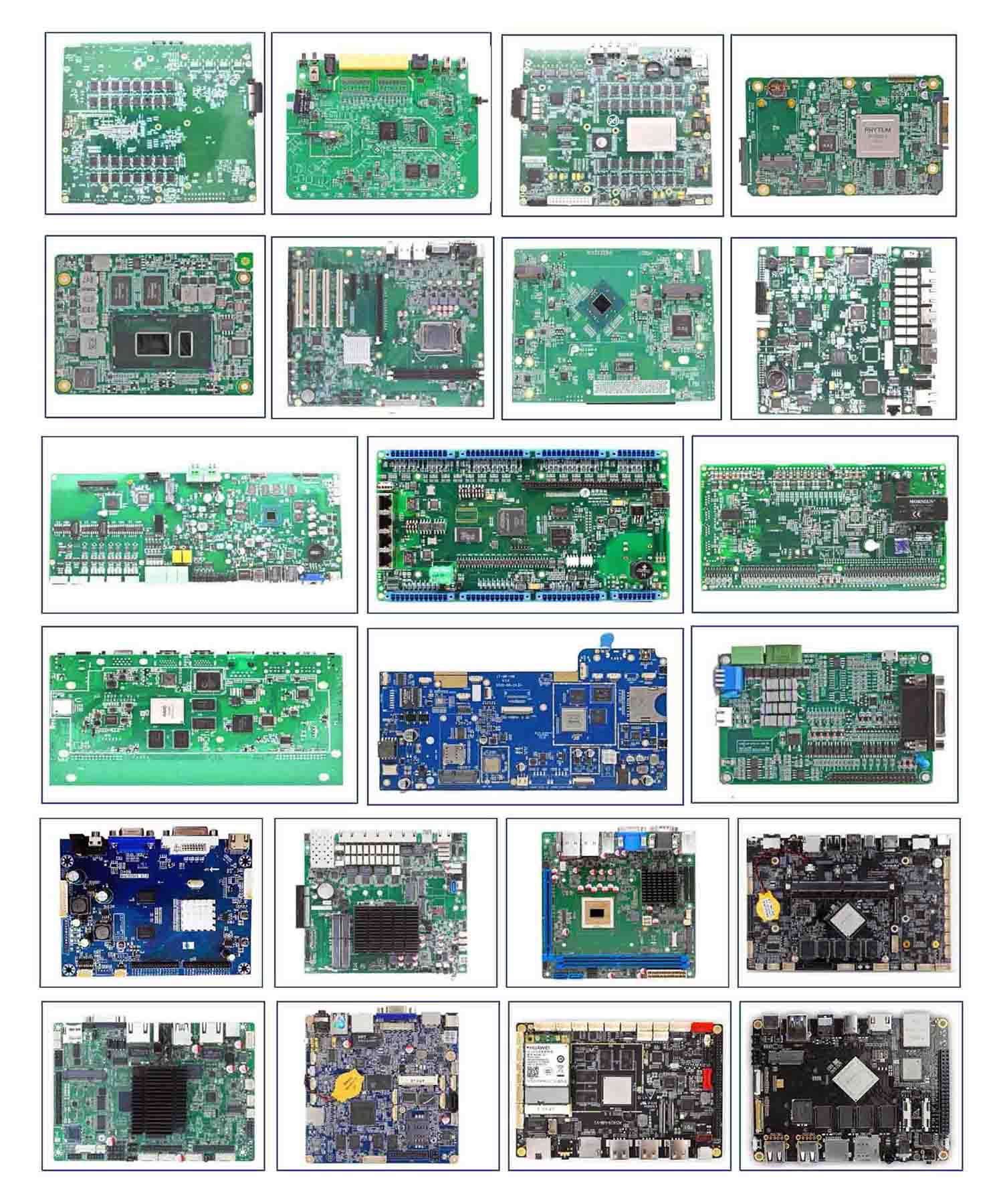
PCB&PCBA Products Show

Certifications
Packaging & Shipping
Packing details:
PCBA are packed into plastic bags. Plastic bags are put into small
carton. 4 small carton into a big carton.
A big carton: 35×32×40 cm size.
Shipping Express:
FedEx, DHL, UPS, TNT, EMS, private lines, etc.
Air freight, Sea shipping

If you need help on PCB layout, you can contact us and send the
board to us. We also provide Reverse Engineering Service.
We have been providing PCB Manufacture for many years in China,and
we have rich experience in product production and product
assembly.We believe our team will provide high quality and low cost
service for you.
Thank you very much for all your support .
Best Regareds.
AFQ:
A:Yes we are manufacturer
Q:Do you provide samples?
A:Yes we can provide free samples,price and shipping cost open for
negotiation
Q:How do you ensure the quality of your products
A:We will burn into file and test the product and ship it after
confirming that there is no problem
Q:What certificates does this product have
A:We have CE,FCC,ROHS certified
Q:What about OEM and ODM?
A:We accept OEM and ODM orders,MOQ is open for discussion
Q:What is delivery terms and time?
A:We use FOB terms and ship the goods in 7-30days depend on your
order quanlity,customization


