Many users of printed circuit boards have found ceramic plates to
be superior to conventional boards made from other materials. This
is because they provide a suitable substrate for electronic
circuits having high thermal conductivity and low coefficient of
expansion (CTE). Multi-layer ceramic PCBs are extremely versatile
and can replace complete traditional printed circuit boards with
simple design and higher performance. Ceramic materials play a key
role in electronic components.
Ceramic substrates such as aluminum oxide, aluminum nitride, and
tantalum oxide are highly thermally conductive materials that
rapidly and efficiently transfer heat away from hot spots to
dissipate heat throughout the surface. PCB material (FR-4) is epoxy
based and has poor thermal conductivity leading to hot spots, which
reduces the lifetime of most semiconductor junctions.
In addition to the enviable thermal properties and coefficient of
expansion, ceramic circuit board can operate at operating
temperatures up to 350 degrees Celsius, resulting in smaller
package sizes, better high frequency performance, and a sealed
package that does not absorb water.
According to different manufacturing methods, there are currently
three basic types of ceramic PCB plates:
A) Thick film ceramic PCB Board
Thick film ceramic PCB: With this technology, the thickness of the
conductor layer exceeds 10 microns, which is thicker than the spray
technology. The conductor is silver or gold palladium and is
printed on a ceramic substrate. More thick film ceramic PCB.
B) Thin film ceramic PCB
Thin film technology ceramic PCB: Since the thickness of the
resistor and the conductor film is less than 10 μm and the film is
sprayed on the ceramic substrate, it is named as a thin film
ceramic plate. More suitable for thin film ceramic PCB.
C) DCB ceramic PCB
The DCB (Direct Copper Bonding) technique represents a special
process in which a copper foil and a core (Al2O3 or AlN) are bonded
directly on one or both sides at a suitable elevated temperature
and pressure. More DCB ceramic PCB.
Materials - Aluminum Nitride and Alumina
Ceramic PCBs are usually made of metal cores. For high thermal
conductivity, aluminum nitride sheets are ideal for providing over
150 w / mK. However, due to the high price of aluminum nitride
sheets, those who choose cheaper ceramic PCBs may find themselves
using alumina sheets, which provide about 18-36w / mK. Both types
will provide better thermal performance than metal core printed
circuit boards because no electrical layer is required between the
core and the circuit.
The use of silver as a print mark - covered with glass for
protection - will further increase the thermal conductivity (406 W
/ mK). Other ceramic material options include boron nitride,
tantalum oxide and silicon carbide. Due to the high operating
temperature, the ceramic plates are not finished with OSP, HASL or
other conventional surface treatments. However, if silver corrosion
can be a problem, such as in a high sulfur environment, you can use
a gold-plated ceramic printed circuit board to protect the exposed
pad.
Ceramic PCB thermal conductivity
High ceramic PCB thermal conductivity may be the main reason why
more industries turn to ceramics in their printed circuit boards
and packages because this material has significant advantages over
plastics in this respect. Better CTE matching and hermetic sealing
will only increase the attractiveness of these materials. The
challenge is that these materials, as well as the boards produced
by ceramic PCB manufacturers, are much more expensive than
traditional printed circuit board materials, and the materials of
traditional printed circuit boards can be greatly increased in
high-volume work. However, the benefits of ceramic plates and the
need to improve thermal conductivity are so great that companies in
any relevant industry that can afford to use ceramic plates may do
so as necessary.
While we can estimate the level of thermal conductivity that each
ceramic plate can provide, the final value will vary depending on
the manufacturing process and the grain size and composition.
The most popular, despite the expensive ceramic - aluminum nitride
- has a thermal conductivity that many people think is more than
150 W / mK, usually about 180 W / mK. However, studies have found
values ranging from 80 W / mK to 200 W / mK at room temperature,
and when approaching 100 degrees Celsius, the value drops by more
than a third. Other thermal ranges that we can identify at room
temperature include alumina of 18-36 W / mK, yttrium oxide of
184-300, boron nitride of 15-600, and silicon carbide of 70-210.
Ceramic PCB application
Industries that require higher frequency connections and good heat
resistance can benefit from ceramic PCBs. The main industries that
ceramic PCBs can serve include: high-power circuits, chip-on-board
modules, aerospace and heavy-duty equipment, automotive, medical
equipment, heavy machinery, high-power transistors and transistor
arrays, solar cell substrates, and other power applications such as
DC conversion. And voltage regulator
PCB advantages:
- R&D team support
- UL, RoHS,ISO9001,SGS
- IPC class2
- Advanced production line and promtly delivery.
- Honest Credibility in China.
- Professional and abundant experience in PCB
- Competitive price and good quality.
- Excellent after-sales service
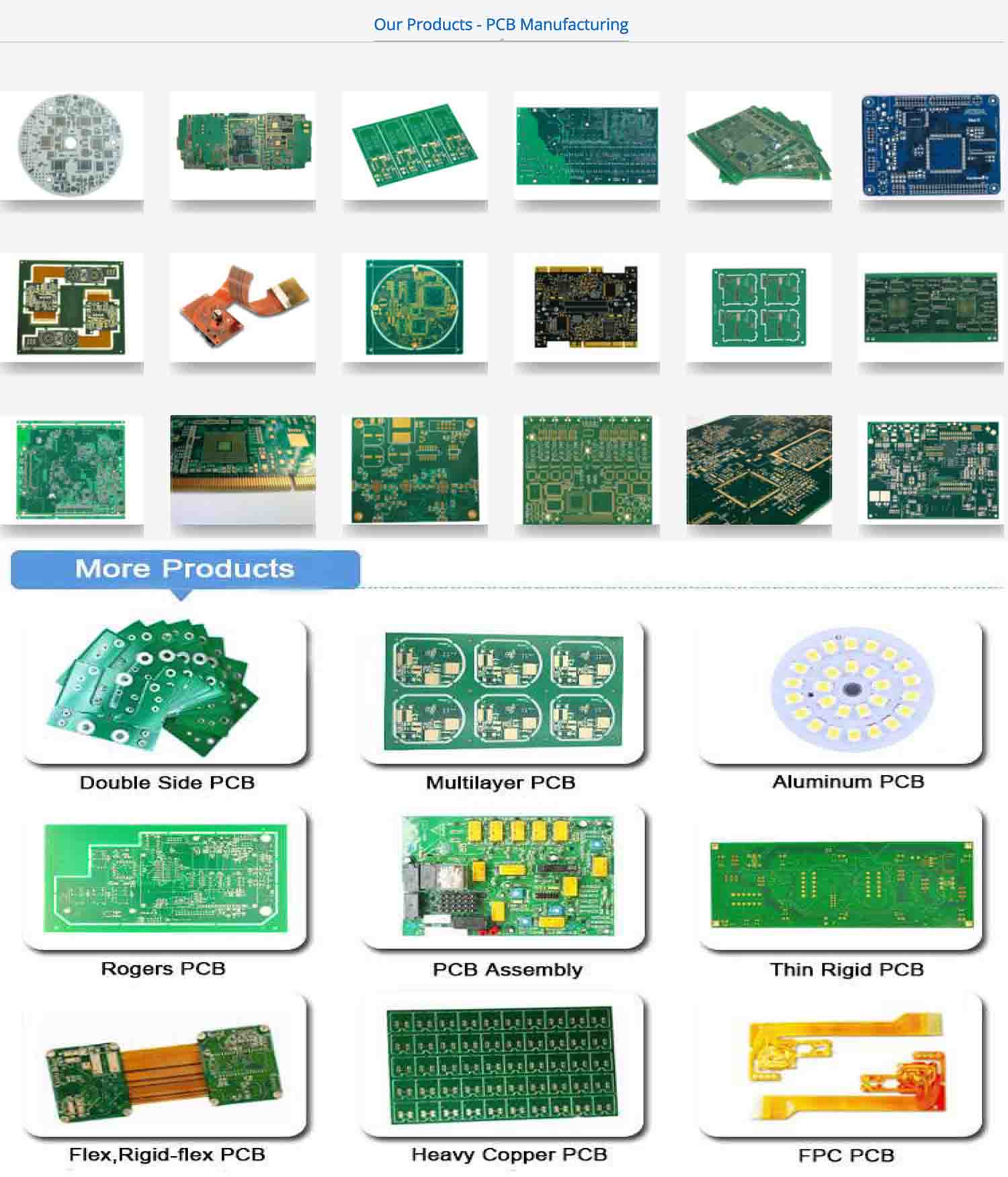
PCB showcase:
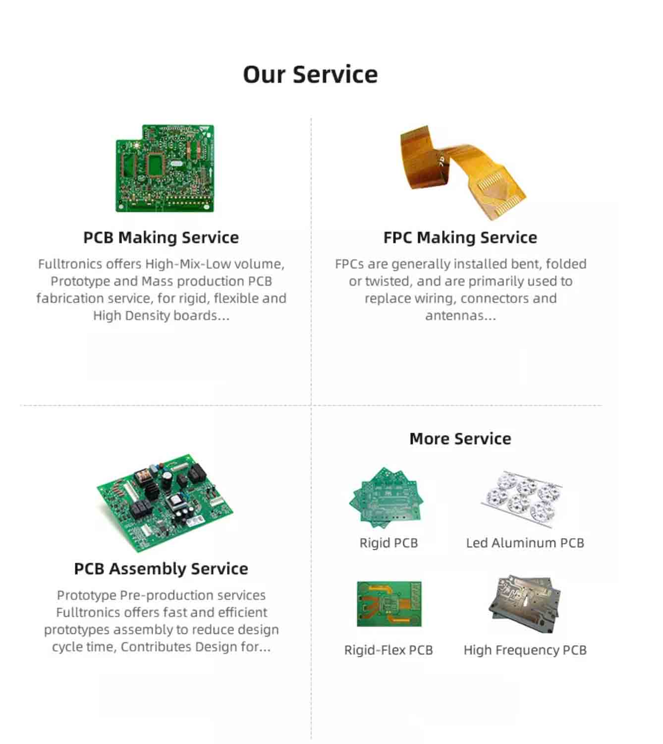
Our Services
1. PCB fabrication.
2. Turnkey PCBA: PCB+components sourcing+SMD and through-hole
assembly
3. PCB clone, PCB reverse engineering.

PCB or PCBA Files Requests:
1. Gerber files of the bare PCB board
2. BOM (Bill of material) for assembly (please kindly advise us if
there is any acceptablecomponents substitution.)
3. Testing Guide & Test Fixtures if necessary
4. Programming files & Programming tool if necessary
5. Schematic if necessary

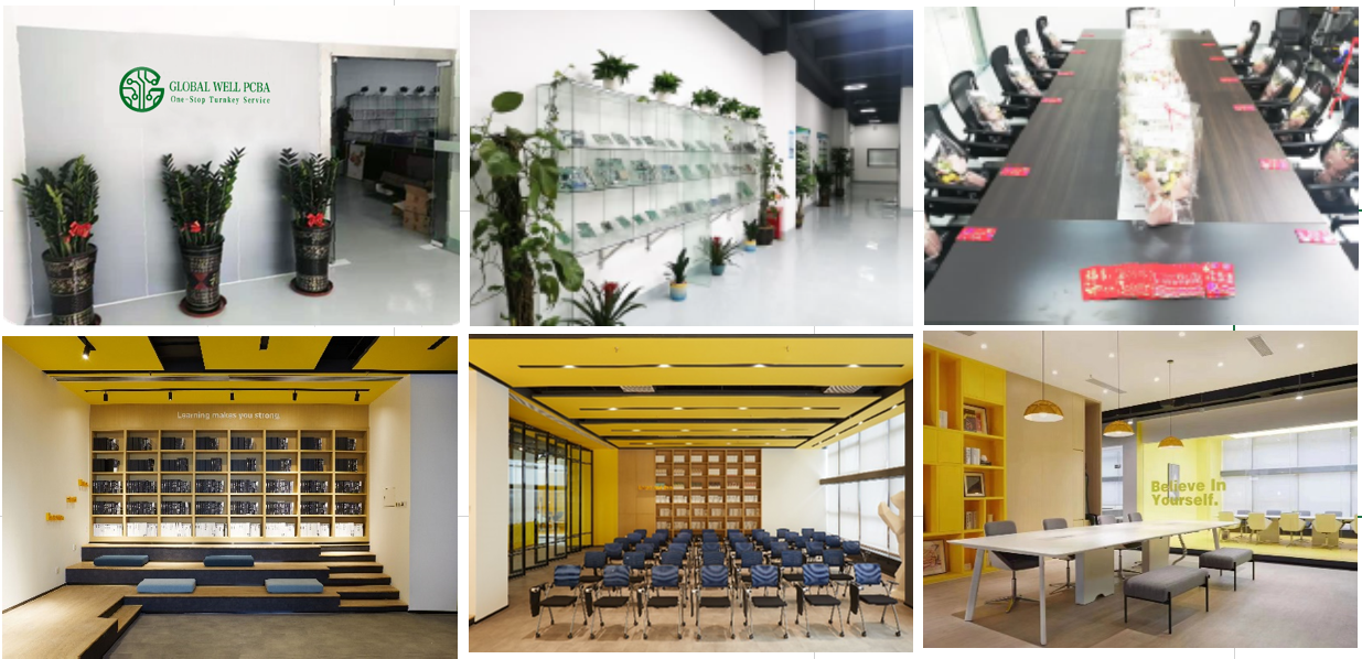
Company Information
Global Well Electronic Inc. is a professional PCB solution supplier
from Shenzhen, China, integrating PCB circuit board production and
processing, STM processing and mounting, PCBA OEM, component
purchasing, PCB/PCBA custom design-production- A comprehensive PCB
circuit board company with one-stop turnkey service of
processing-assembly-finished products. The company has a strong
supply chain system, a professional and efficient collaborative
team, a sound and complete quality control system, and the business
philosophy of honesty and trustworthiness, customer first, and
presents the products to everyone with low prices, reliable
quality, high-quality service and after-sales service. client.
We provide total PCB solutions from PCB design to final mass
production, including PCB fabrication and assembly, component
sourcing, solder paste stencils, conformal coatings, and more.
Serving the global electronics field, including industrial control,
medical electronics, military equipment, power communication,
automotive electronics, AI artificial intelligence, smart home and
other industries.

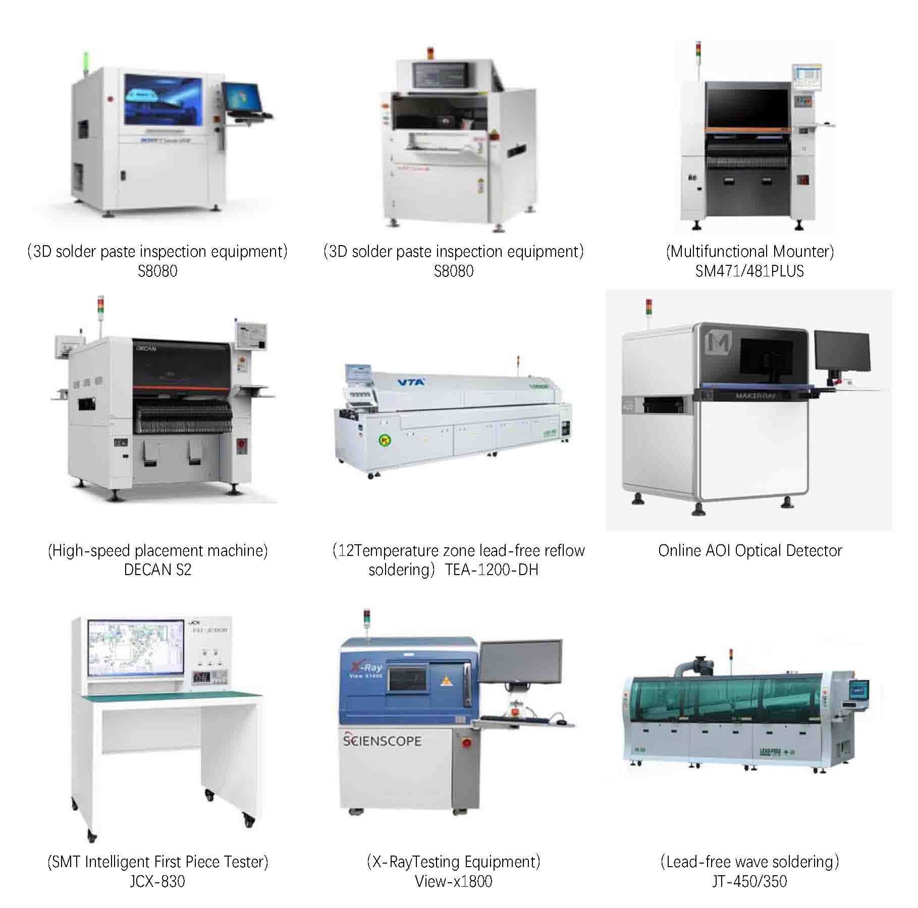
Our factory located in Shenzhen, and have almost 300 employees,
more than 30 production lines include SMT, DIP, automatic welding,
aging test and assembly. We have SMT machines from Japan and Korea,
automatic solder paste printing machines, solder paste inspection
machine(SPI)12 temperature zone reflow soldering machine, AOI
detector, X-RAY detector, wave soldering machine, EM PCB
,dispenser,laser print machine etc., Different line configurations
can meet requirements from small sample order to bulk shipment.
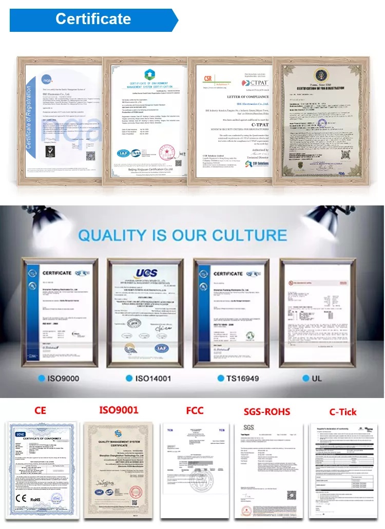
Our company has obtained ISO 9001 quality system certification and
ISO 14001 system certification. With multi-testingprocedures, our
products carry out the quality system standard strictly.
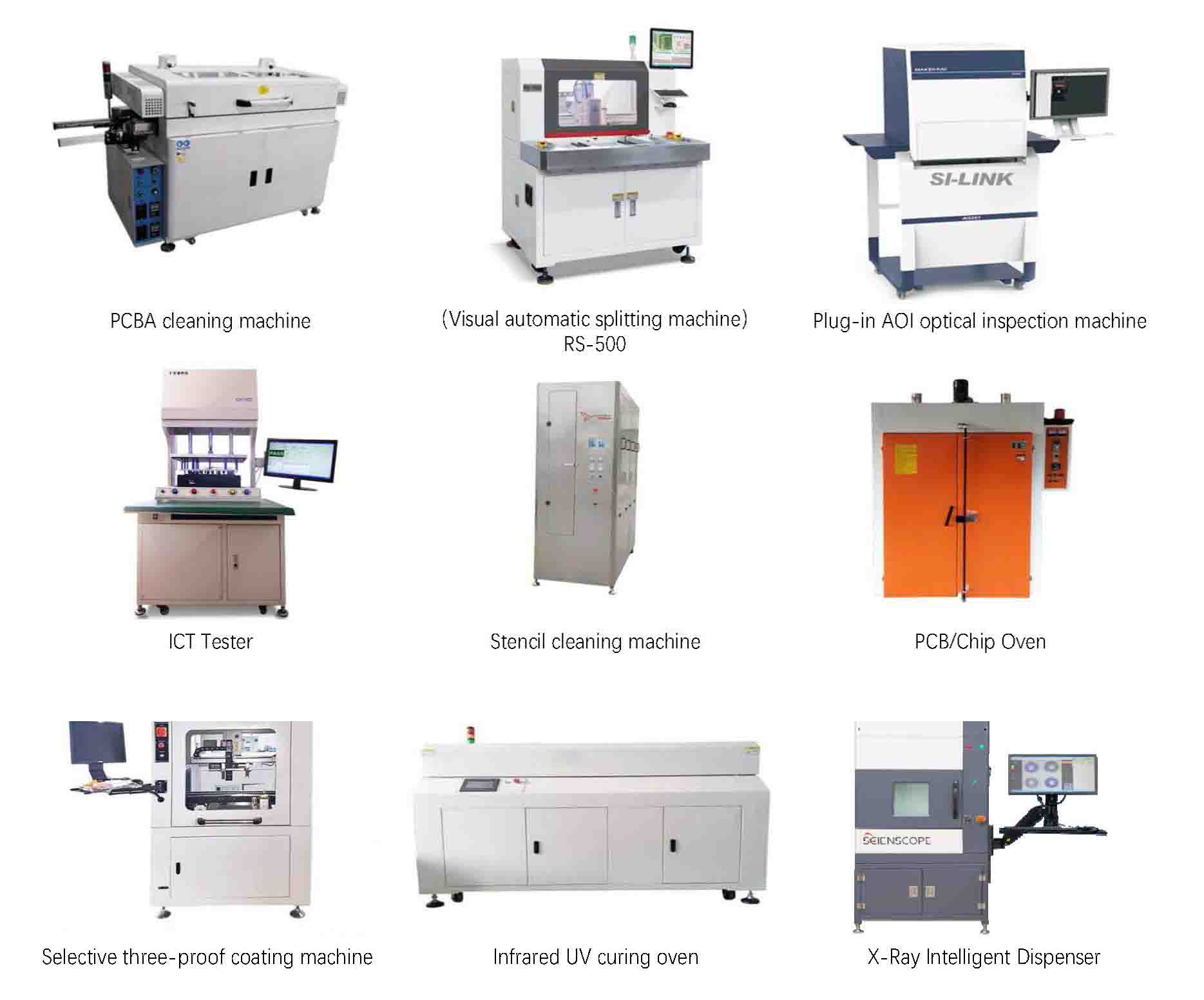
Main Equipment:

PCB Technical Specification
(1) PCB Technical Specification
| Order Quantity | 1-300,000,30000 Square Meter/Square Meters per Month module
electronic board |
| Layer | 1,2,4,6,upto 40 layer |
| Material | FR-4,glass epoxy,FR4 High Tg,Rohs compliant,Aluminum,Rogers,etc |
| PCB type | Rigid,flexible,rigid-flexible |
| Shape | Any shape: Rectangular,round,slots,cutouts,complex,irregular |
| Max PCB dimensions | 20inch*20inch or 500mm*500mm |
| Thickness | 0.2~4.0mm, Flex 0.01~0.25'' |
| Thickness tolerance | ± 10% |
| Copper thickness | 0.5-4 oz |
| Copper thickness tolerance | ± 0.25oz |
| Surface finish | HASL,Nickle,Imm Gold,Imm Tin,Imm Silver,OSP etc |
| Solder mask | Green, red,white,yellow,blue,black, Double-sided |
| Silk screen | White,yellow,black,or negative, Double-sided or single-sided |
| Silk screen min line width | 0.006'' or 0.15mm |
| Min drill hole diameter | 0.01'',0.25mm.or 10 mil |
| Min trace/gap | 0.075mm or 3mil |
| PCB cutting | Shear,V-score,tab-routed |
(2) Turnkey PCBA Capabilities
| Turnkey PCBA | PCB+components sourcing+assembly+package |
| Assembly details | SMT and Thru-hole, ISO lines |
| Lead Time | Prototype: 15 work days. Mass order: 20~25 work days |
| Testing on products | Flying Probe Test, X-ray Inspection, AOI Test, functional test |
| Quantity | Min quantity: 1pcs. Prototype, small order, mass order, all OK |
| Files we need | PCB: Gerber files(CAM, PCB, PCBDOC) |
| Components: Bill of Materials(BOM list) |
| Assembly: Pick-N-Place file |
| PCB panel Size | Min size: 0.25*0.25 inches(6*6mm) |
| Max size: 20*20 inches(500*500mm) |
| PCB Solder Type | Water Soluble Solder Paste, RoHS lead free |
| Components details | Passive Down to 0201 size |
| BGA and VFBGA |
| Leadless Chip Carriers/CSP |
| Double-sided SMT Assembly |
| Fine Pitch to 0.8mils |
| BGA Repair and Reball |
| Part Removal and Replacement |
| Component package | Cut Tape,Tube,Reels,Loose Parts |
| PCBA process | Drilling-----Exposure-----Plating-----Etaching Stripping-----Punching-----Electrical Testing-----SMT-----Wave Soldering-----Assembling-----ICT-----Function
Testing-----Temperature - Humidity Testing |
PCB&PCBA Products Show


Company Certifications
Packaging & Shipping
Packing details:
PCBA are packed into plastic bags. Plastic bags are put into small
carton. 4 small carton into a big carton.
A big carton: 35×32×40 cm size.
Shipping Express:
FedEx, DHL, UPS, TNT, EMS, private lines, etc.
Air freight, Sea shipping

If you need help on PCB layout, you can contact us and send the
board to us. We also provide Reverse Engineering Service.
We have been providing PCB Manufacture for many years in China,and
we have rich experience in product production and product
assembly.We believe our team will provide high quality and low cost
service for you.
Thank you very much for all your support .
Best Regareds.
AFQ:
A:Yes we are manufacturer
Q:Do you provide samples?
A:Yes we can provide free samples,price and shipping cost open for
negotiation
Q:How do you ensure the quality of your products
A:We will burn into file and test the product and ship it after
confirming that there is no problem
Q:What certificates does this product have
A:We have CE,FCC,ROHS certified
Q:What about OEM and ODM?
A:We accept OEM and ODM orders,MOQ is open for discussion
Q:What is delivery terms and time?
A:We use FOB terms and ship the goods in 7-30days depend on your
order quanlity,customization