1. PCB fabrication.
2. Turnkey PCBA: PCB+components sourcing+SMD and through-hole
assembly
3. PCB clone, PCB reverse engineering.

PCB or PCBA Files Requests:
1. Gerber files of the bare PCB board
2. BOM (Bill of material) for assembly (please kindly advise us if
there is any acceptablecomponents substitution.)
3. Testing Guide & Test Fixtures if necessary
4. Programming files & Programming tool if necessary
5. Schematic if necessary
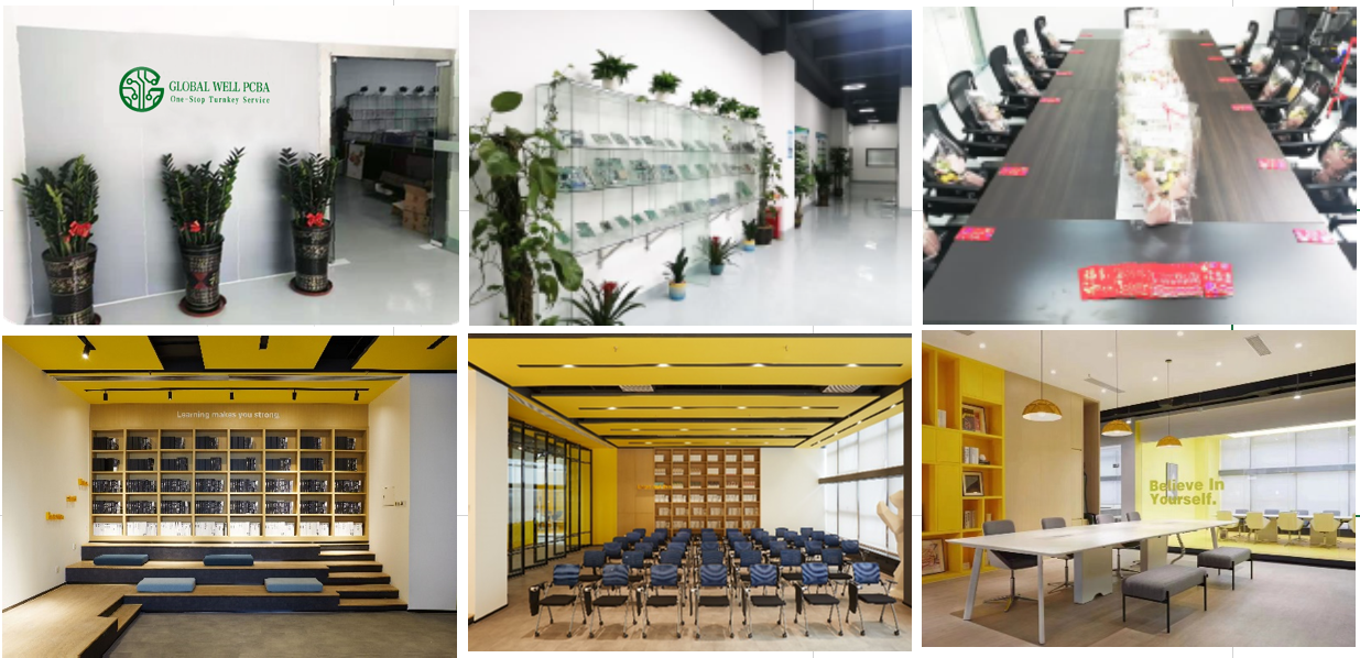
Company Information
Global Well Electronic Inc. is a professional PCB solution supplier
from Shenzhen, China, integrating PCB circuit board production and
processing, STM processing and mounting, PCBA OEM, component
purchasing, PCB/PCBA custom design-production- A comprehensive PCB
circuit board company with one-stop turnkey service of
processing-assembly-finished products. The company has a strong
supply chain system, a professional and efficient collaborative
team, a sound and complete quality control system, and the business
philosophy of honesty and trustworthiness, customer first, and
presents the products to everyone with low prices, reliable
quality, high-quality service and after-sales service. client.
We provide total PCB solutions from PCB design to final mass
production, including PCB fabrication and assembly, component
sourcing, solder paste stencils, conformal coatings, and more.
Serving the global electronics field, including industrial control,
medical electronics, military equipment, power communication,
automotive electronics, AI artificial intelligence, smart home and
other industries.

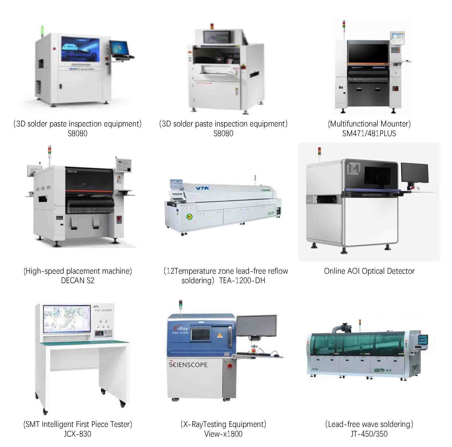
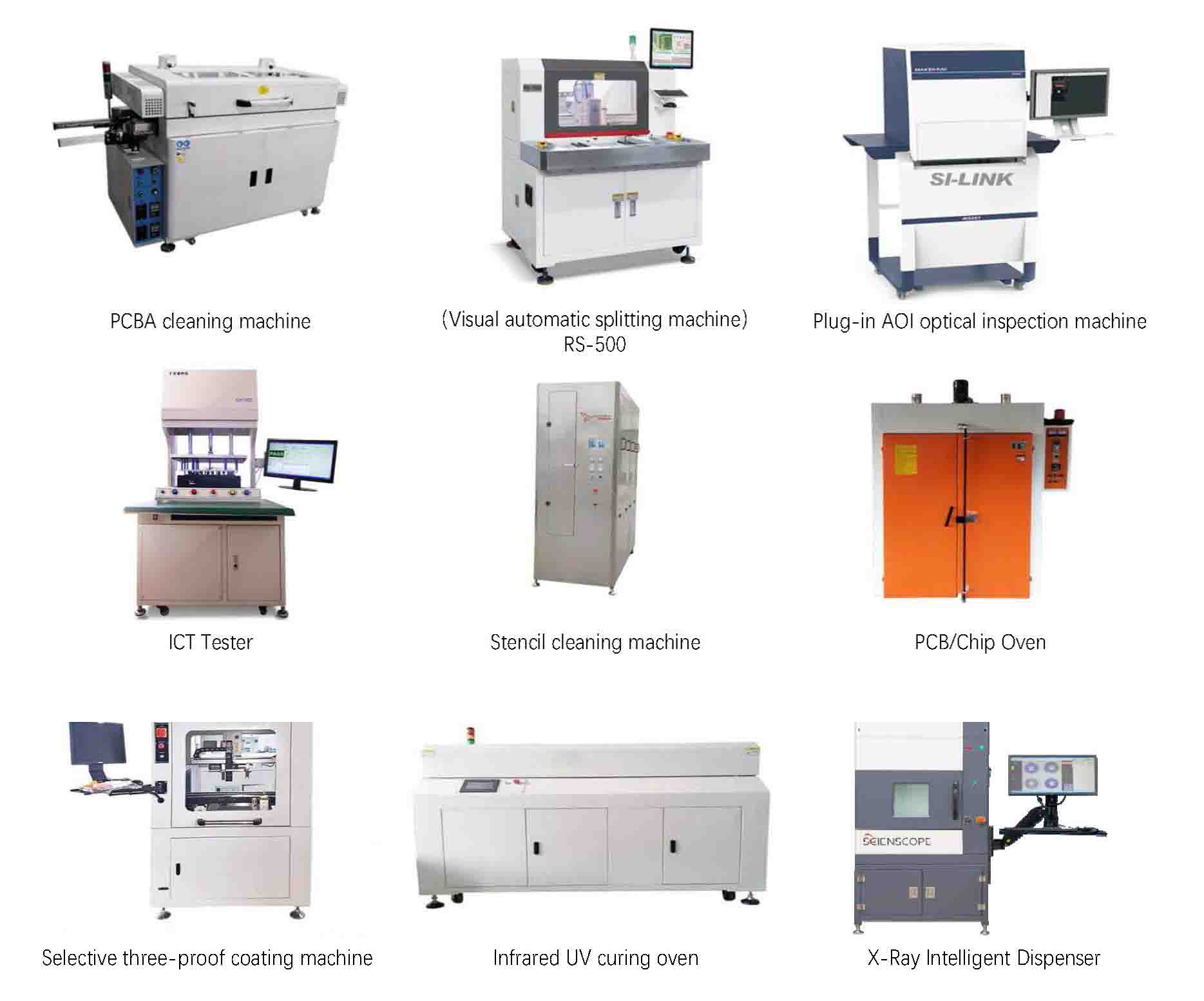
Our factory located in Shenzhen, and have almost 300 employees,
more than 30 production lines include SMT, DIP, automatic welding,
aging test and assembly. We have SMT machines from Japan and Korea,
automatic solder paste printing machines, solder paste inspection
machine(SPI)12 temperature zone reflow soldering machine, AOI
detector, X-RAY detector, wave soldering machine, EM PCB
,dispenser,laser print machine etc., Different line configurations
can meet requirements from small sample order to bulk shipment.
Our company has obtained ISO 9001 quality system certification and
ISO 14001 system certification. With multi-testingprocedures, our
products carry out the quality system standard strictly.
Main Equipment:

Company Capabilities
(1) PCB Technical Specification
| Order Quantity | 1-300,000,30000 Square Meter/Square Meters per Month module
electronic board |
| Layer | 1,2,4,6,upto 40 layer |
| Material | FR-4,glass epoxy,FR4 High Tg,Rohs compliant,Aluminum,Rogers,etc |
| PCB type | Rigid,flexible,rigid-flexible |
| Shape | Any shape: Rectangular,round,slots,cutouts,complex,irregular |
| Max PCB dimensions | 20inch*20inch or 500mm*500mm |
| Thickness | 0.2~4.0mm, Flex 0.01~0.25'' |
| Thickness tolerance | ± 10% |
| Copper thickness | 0.5-4 oz |
| Copper thickness tolerance | ± 0.25oz |
| Surface finish | HASL,Nickle,Imm Gold,Imm Tin,Imm Silver,OSP etc |
| Solder mask | Green, red,white,yellow,blue,black, Double-sided |
| Silk screen | White,yellow,black,or negative, Double-sided or single-sided |
| Silk screen min line width | 0.006'' or 0.15mm |
| Min drill hole diameter | 0.01'',0.25mm.or 10 mil |
| Min trace/gap | 0.075mm or 3mil |
| PCB cutting | Shear,V-score,tab-routed |
(2) Turnkey PCBA Capabilities
| Turnkey PCBA | PCB+components sourcing+assembly+package |
| Assembly details | SMT and Thru-hole, ISO lines |
| Lead Time | Prototype: 15 work days. Mass order: 20~25 work days |
| Testing on products | Flying Probe Test, X-ray Inspection, AOI Test, functional test |
| Quantity | Min quantity: 1pcs. Prototype, small order, mass order, all OK |
| Files we need | PCB: Gerber files(CAM, PCB, PCBDOC) |
| Components: Bill of Materials(BOM list) |
| Assembly: Pick-N-Place file |
| PCB panel Size | Min size: 0.25*0.25 inches(6*6mm) |
| Max size: 20*20 inches(500*500mm) |
| PCB Solder Type | Water Soluble Solder Paste, RoHS lead free |
| Components details | Passive Down to 0201 size |
| BGA and VFBGA |
| Leadless Chip Carriers/CSP |
| Double-sided SMT Assembly |
| Fine Pitch to 0.8mils |
| BGA Repair and Reball |
| Part Removal and Replacement |
| Component package | Cut Tape,Tube,Reels,Loose Parts |
| PCBA process | Drilling-----Exposure-----Plating-----Etaching Stripping-----Punching-----Electrical Testing-----SMT-----Wave Soldering-----Assembling-----ICT-----Function
Testing-----Temperature - Humidity Testing |
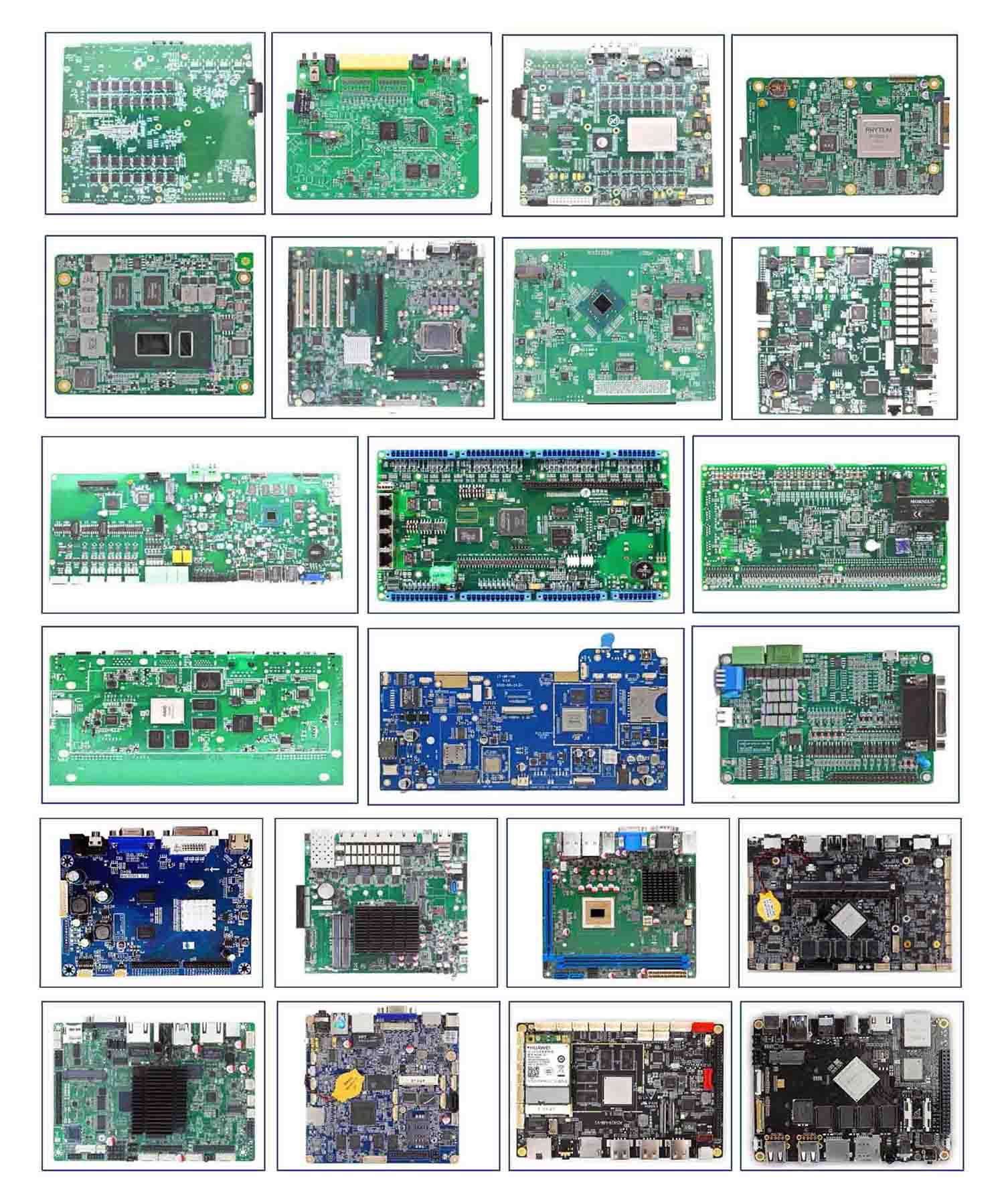
PCB&PCBA Products Show
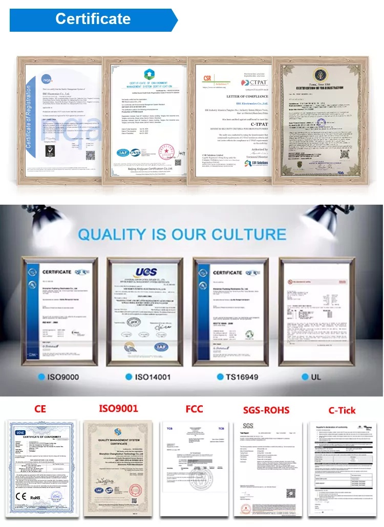
Certifications
Packaging & Shipping
Packing details:
PCBA are packed into plastic bags. Plastic bags are put into small
carton. 4 small carton into a big carton.
A big carton: 35×32×40 cm size.
Shipping Express:
FedEx, DHL, UPS, TNT, EMS, private lines, etc.
Air freight, Sea shipping

If you need help on PCB layout, you can contact us and send the
board to us. We also provide Reverse Engineering Service.
We have been providing PCB Manufacture for many years in China,and
we have rich experience in product production and product
assembly.We believe our team will provide high quality and low cost
service for you.
Thank you very much for all your support .
Best Regareds.
AFQ:


